TOP > NCKU GICRC-Semiconductor Division
 |
Prof. Takayuki OHBA(Specially Appointed)(Concurrent Post) | |||
| Room | S9 | Mail-Box | S9-11 | |
| TEL | 03-5734-2211 | |||
| takayuki.ohba(at)first.iir.isct.ac.jp Please replace “(at)” with “@”. | ||||
| HomePage | https://www.wow.first.iir.isct.ac.jp/ | |||
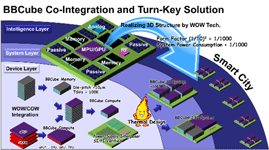
| Research Field | BBCube LSI Semiconductor Process Development and Applications | |||
| Objective | To develop the cutting-edge BBCube three-dimensional large-scale integration technology and drive the semiconductor industry beyond scaling. | |||
| Current Topics |
|
|||
 |
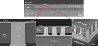 |
| Bumpless vertical interconnects between wafers | |
 |
Prof. Kuan-Neng CHEN(Specially Appointed)〔Ito Lab〕(Concurrent Post) | |||
| Room | J3 | Mail-Box | J3-132 | |
| TEL | 045-924-5866 | |||
| chien.k.0dea(at)m.isct.ac.jp Please replace “(at)” with “@”. | ||||
| HomePage | ||||
 |
Prof. Norio CHUJO(Specially Appointed)〔Ito Lab〕(Concurrent Post) | |||
| Room | R2棟 | Mail-Box | R2-32 | |
| TEL | 045-924-5083 | |||
| chuujou.n.813f(at)m.isct.ac.jp Please replace “(at)” with “@”. | ||||
| HomePage | https://www.wow.first.iir.isct.ac.jp/ | |||
| Research Field | Design and architecture of BBCube 3D integration | |||
| Objective | Development of semiconductor technologies that achieve both high performance and low. | |||
| Current Topics |
|
|||
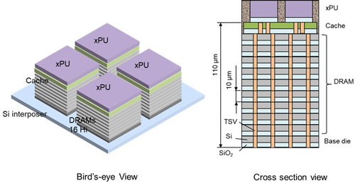 |
| BBCube 3D configuration ・Multi-xPU/IVR/Multi-Memory Vertical Stack ・WOW and COW Hybrid Processes ・Cu-Damascene Via-Last TSVs) |
 |
Prof. Takashi YODA(Specially Appointed)〔Ohba Lab〕(Concurrent Post) | |||
| Room | R2棟 | Mail-Box | R2-32 | |
| TEL | 045-924-5083 | |||
| takashi.yoda(at)first.iir.isct.ac.jp Please replace “(at)” with “@”. | ||||
| HomePage | https://www.wow.first.iir.isct.ac.jp/ | |||
| Research Field | Wide Band Gap (WBG) Semiconductor Technology | |||
| Objective | Development of the High performance SiC/(GaN) devices | |||
| Current Topics |
|
|||
 |
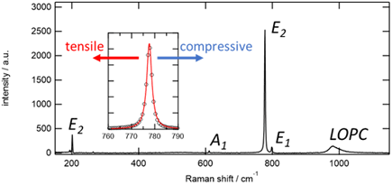 |
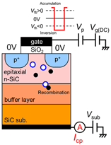
| Lifetime measurement for n-Buffer SiC layer | Hyperspectral Raman Imaging of 4H-SiC BPD |
 |
Prof. Young Suk KIM(Visiting)〔Ito Lab〕(Concurrent Post) | |||
| Room | J3 | Mail-Box | J3-132 | |
| TEL | 045-924-5866 | |||
| youngsuk.k.aa(at)m.titech.ac.jp Please replace “(at)” with “@”. | ||||
| HomePage | http://www.wow.pi.titech.ac.jp/ | |||
| Research Field | Process Integration Development for 3D LSI Devices | |||
| Objective | To develop ultra-thinning of 300-mm device wafers and those stack process integration technology for three-dimensional LSI technology. Because the physical interconnects length becomes 1/10 using ultra-thin wafers and Wafer-on-Wafer (WOW) process, high performance 3D devices with low power consumption will be realized. | |||
| Current Topics |
|
|||
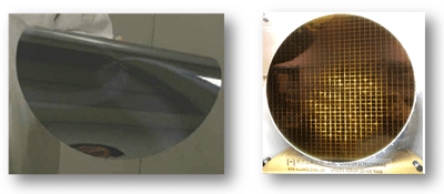
Thinned DRAM 300mm wafer
国立大学法人東京科学大学
総合研究院 未来産業技術研究所
Laboratory for Future Interdisciplinary Research of Science and Technology (FIRST),
Institute of Integrated Research (IIR),
Institute of Science Tokyo
 MAP
MAP
Copyright (C) Institute of Science Tokyo. All rights reserved.



 このページの先頭へ